
")
")
")
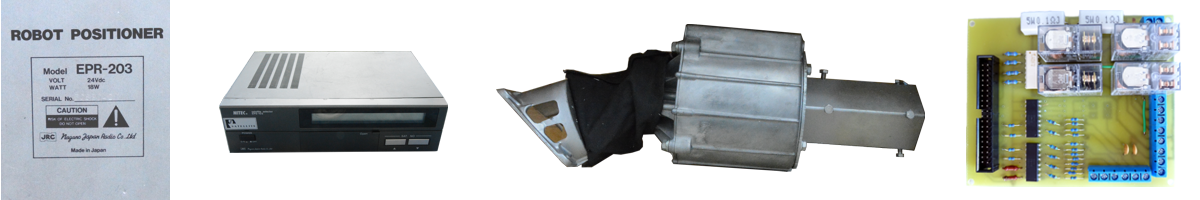
HW 2.1 design
I started working on the circuit board. I have set the following conditions that I would like to adhere to:
- The overall dimensions of the printed circuit board are not important. But I would like to get closer to the dimensions of the first version, i.e. 110 mm x 90 mm.
- Place the individual components into logical units. For example, place the terminal blocks of individual functional blocks next to each other if possible. Place the L6203 circuits so that they can all be attached to one common heatsink.
- If possible, use a PCB with only two layers.
- The density of connections on the board in a grid of 2.5 mm.
- No need to use SMD components.
The intention is that the printed circuit board can be made at home in amateur conditions.
I drew the diagram in Eagle 8.2.0. However, I have not been able to arrange the components on the printed circuit board so far. That's why I put the schematic in the Files for download / For HW version 2.1 section. There you can download it and try to design the PCB yourself. I'd love to hear from any of you who have had success with the PCB design. And made it available to others through my website.